4H SiC Wafer
The mainstream SiC polytype for power MOSFETs, Schottky diodes and high-voltage modules. Low defectivity substrates, epi-ready Si-face CMP polish, and tight bow/TTV deliver high yields for thick-epi power stacks.
- Samples in 3–7 days
- Small batch in ~7 days
- 1 pc MOQ
4H SIC Crystal Structure Overview
Zirsec 4H-SiC wafers are designed for high-performance applications with industry-leading electrical properties, thermal conductivity, and mechanical strength.
SiC is a crystal composed of silicon (Si) and carbon (C) in a 1:1 stoichiometric ratio. Due to differences in the internal structural stacking sequence, various SiC polytypes are formed.
Currently, the 4H-SiC and 6H-SiC polytypes are the most common and widely used. The 4h sic wafer is a key factor that enables SiC-based devices to perform excellently in high-power, high-frequency, and high-temperature applications.
With its hexagonal lattice structure, high breakdown voltage, excellent thermal conductivity, and wide bandgap, 4H-SiC is widely used in advanced semiconductor devices, including power electronics, RF devices, and high-temperature environments. It is indispensable in industries such as electric vehicles, aerospace, and renewable energy.
FEATURES & BENEFITS
- High Breakdown Voltage: Ideal for high-voltage semiconductors
- Thermal Conductivity: Effective heat dissipation
- High Electron Mobility: Fast switching and high-frequency efficiency
- Mechanical Strength: Strong and heat-resistant
- Wide Bandgap: Works in high-temperature conditions
APPLICATIONS AREAS
- Power Electronics: MOSFETs, diodes, IGBTs
- RF Devices: Radar and communications
- High-Temperature: Aerospace and automotive
- Optoelectronics: LEDs and laser diodes
4H SIC Wafer Properties
| Property | Single Crystal 4H |
| Lattice Parameters | a = 3.076 Å, c = 10.053 Å |
| Crystal Sequence | ABCB |
| Band Gap | 3.26 eV |
| Density | 3.21 × 10³ kg/m³ |
| Thermal Expansion Coefficient | 4-5×10⁻⁶ /K |
| Refractive Index | no = 2.719, ne = 2.777 |
| Dielectric Constant | 9.6 |
| Thermal Conductivity | 490 W/mK |
| Breakdown Electric Field | 2-4 × 10⁸ V/m |
| Sound Wave Propagation Speed | 2.0 × 10⁵ m/s |
| Electron Mobility | 800 cm²/V·s |
| Hole Mobility | 115 cm²/V·s |
| Mohs Hardness | ~9 |
4H Silicon Carbide Specification
| Model | Name | Diameter | Thickness |
| AT-SIC-JP001N | Conductive Silicon Carbide Wafer | 2 inches | 0.35 mm |
| AT-SIC-JP002N | Conductive Silicon Carbide Wafer | 3 inches | 0.35 mm |
| AT-SIC-JP003N | Conductive Silicon Carbide Wafer | 4 inches | 0.35 mm |
| AT-SIC-JP004N | Conductive Silicon Carbide Wafer | 6 inches | 0.35 mm |
| AT-SIC-JP005N | Conductive Silicon Carbide Wafer | 2 inches | 0.5 mm |
| AT-SIC-JP006N | Conductive Silicon Carbide Wafer | 3 inches | 0.5 mm |
| AT-SIC-JP007N | Conductive Silicon Carbide Wafer | 4 inches | 0.5 mm |
| AT-SIC-JP008N | Conductive Silicon Carbide Wafer | 6 inches | 0.5 mm |
| AT-SIC-JP005 | Semi-Insulating Silicon Carbide Wafer | 2 inches | 0.35 mm |
| AT-SIC-JP006 | Semi-Insulating Silicon Carbide Wafer | 3 inches | 0.35 mm |
| AT-SIC-JP007 | Semi-Insulating Silicon Carbide Wafer | 4 inches | 0.35 mm |
| AT-SIC-JP008 | Semi-Insulating Silicon Carbide Wafer | 6 inches | 0.35 mm |
| AT-SIC-JP009 | Semi-Insulating Silicon Carbide Wafer | 2 inches | 0.5 mm |
| AT-SIC-JP010 | Semi-Insulating Silicon Carbide Wafer | 3 inches | 0.5 mm |
| AT-SIC-JP011 | Semi-Insulating Silicon Carbide Wafer | 4 inches | 0.5 mm |
| AT-SIC-JP012 | Semi-Insulating Silicon Carbide Wafer | 6 inches | 0.5 mm |
Specifications of 4H SIC Wafer Packaging Box
| Name | Model | Wafer Size Capacity |
| Wafer Single Piece Box | 1 inch | Approximately 25mm diameter wafer |
| 2 inch | Approximately 50mm diameter wafer | |
| 3 inch | Approximately 76mm diameter wafer | |
| 4 inch | Approximately 100mm diameter wafer | |
| 6 inch | Approximately 150mm diameter wafer | |
| 8 inch | Approximately 200mm diameter wafer |

Custom 4H Silicon Carbide Wafers
Zirsec offers full customization of 4H Silicon Carbide wafers to meet your specific needs. Our team works closely with you to deliver the exact specifications required for your application.
Diameter
Available in 2 inches, 3 inches, 4 inches, and 6 inches. Custom sizes available upon request.
Thickness
Standard thickness: 0.35 mm, 0.5 mm. -Other thicknesses are available.
Doping Type
Conductive (N-type, P-type) ;Semi-Insulating
Polishing and Surface Quality
High-quality polished wafers with minimal defects for optimal performance.
Crystal Orientation
Customized crystal orientation options, including specific alignment to suit your application.
FAQ
1) Why 4° off-axis?
It promotes step-flow epitaxy and suppresses polytype inclusions for thick power epi growth.
2) Typical thickness and diameters?
2/3/4″ at 350 μm for N-type and 500 μm for SI; 6″ N-type at 350 μm common.
3) What MPD do you offer?
Prime grade targets ≤1 cm⁻²; production/research grades up to 5–15 cm⁻² depending on cost.
4) Surface quality?
5) Electrical ranges?
N-type ~0.015–0.028 Ω·cm; semi-insulating >1×10⁵ Ω·cm. We bin by resistivity and map uniformity.
6) Standards?
SEMI M55 for dimensions; SEMI M81 for defect terminology and inspection guides.
7) Can you support 150 mm and 200 mm?
8) Application focus for 4H vs 6H?
9) Do you provide epi or test coupons?
10) Packaging and marking?


Customization
From design to reverse engineering, we provide free technical consulting to help upgrade your equipment. We specialize in high-precision complex parts with ±0.01mm tolerances and special coatings like acid and oxidation resistance, tailored for demanding industrial applications.
FAQ
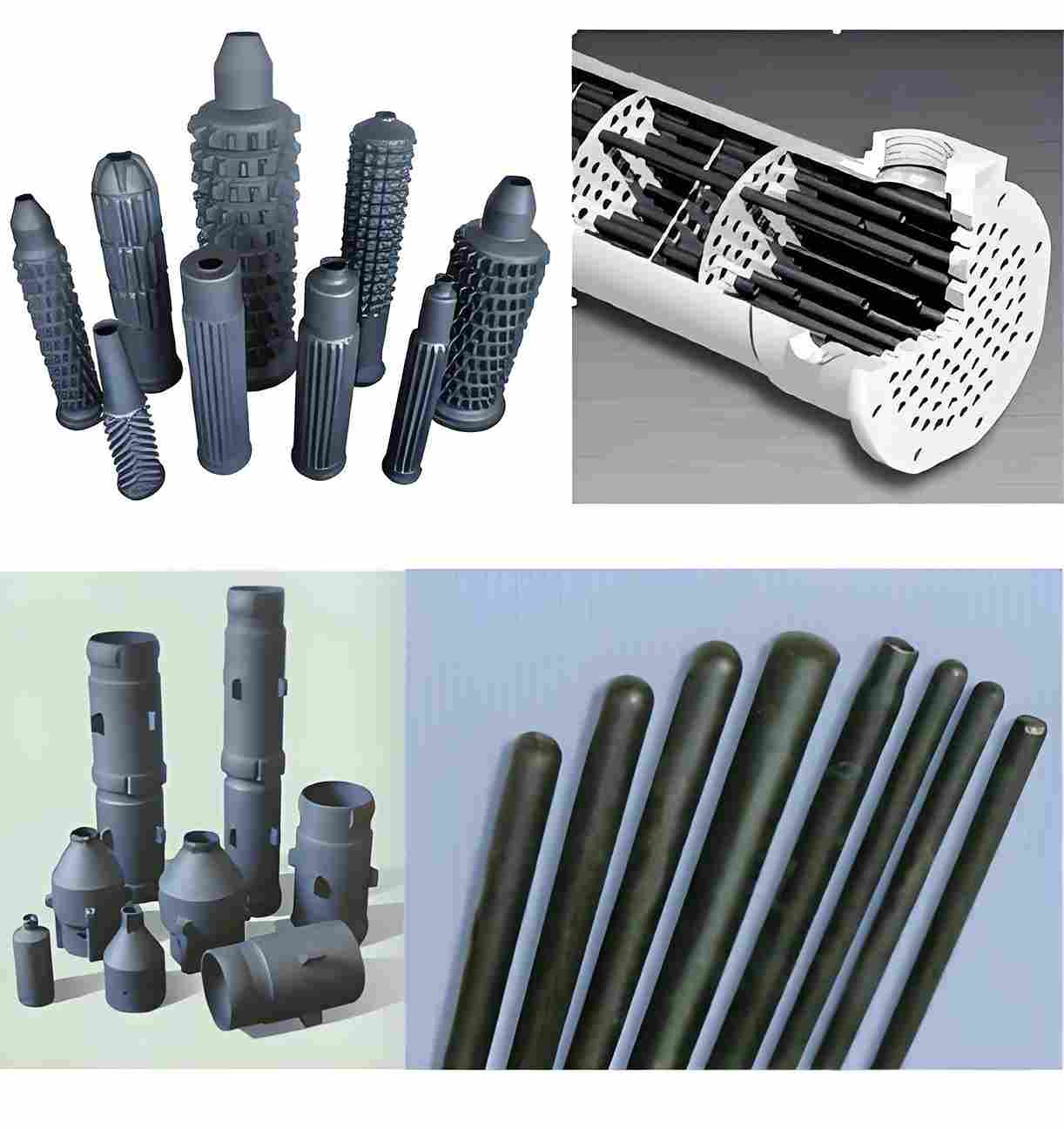
What types of silicon carbide products does Zirsec supply?
Zirsec offers a wide range of SiC components including tubes, beams, plates, crucibles, rollers, sealing rings, and custom mechanical parts for industrial, chemical, and semiconductor applications.
Can Zirsec provide customized sizes or shapes?
Yes. We support OEM and customized production based on your drawings, specifications, or working conditions.
Do you provide samples for testing?
Yes, sample orders are available for standard items. For custom-made components, small batch samples can be produced after design confirmation.
How can I request a quotation?
Simply fill out the contact form on this page with product type, quantity, and specifications. Our sales engineer will send you a detailed quotation within 24 hours.
Does Zirsec offer technical consultation or design assistance?
Absolutely. Our engineers provide material selection guidance, structural optimization, and technical support for your specific applications.
How does Zirsec ensure product quality?
All products undergo strict inspection procedures, including dimensional accuracy, density, strength, and corrosion resistance tests before delivery.
Tell us your requirements
Our technical engineer will reply with a custom solution and quotation within one working day.