Wafers and Substrates Silicon Carbide – Zirsec")
Silicon Carbide (SiC) Wafers & Substrates
Epi-ready 4H/6H SiC substrates for power devices, RF/MMIC, and harsh-environment sensing. Tight geometry per SEMI M55, low defect density, and controlled bow/TTV to drive yield and reliability.
- Samples in 3–7 days
- Small batch in ~7 days
- 1 pc MOQ
Silicon Carbide Wafer Manufacturer
Zirsec supplies high-quality 4H-Silicon Carbide and 6H-Silicon Carbide wafers, available in both conductive and semi-insulating types. Our wafers feature low defect density, excellent thermal performance, and precise doping control, making them ideal for power and RF device applications.
We also provide Silicon Carbide substrates with superior crystal quality and surface finish, supporting epitaxial growth and high-reliability chip production. With full customization and stable supply, Zirsec powers your next-generation semiconductor solutions.
Silicon Carbide Properties | Available Polytypes
4H-SiC | 6H-SiC | |
|---|---|---|
| Diameter | 50mm (2″), 76mm (3″), 100mm (4″), 150mm (6″) | 50mm (2″) & 100mm (4″) |
| Type/Dopant | N/Nitrogen / intrinsic / HPSI | N/Nitrogen / intrinsic / HPSI |
| Resistivity | .012 – .028 ohm*cm | >.00001 ohm*cm |
| Thickness | 250um – 15,000um (15mm) | 250um – 15,000um (15mm) |
| Surface Finish | Single or double side polished | Single or double side polished |
| Stacking Sequence | ABCB | ABCACB |
| Dielectric Constant | 9.6 | 9.66 |
| Electron Mobility | 800 cm2/V*S | 400 cm2/V*S |
| Density | 3.21 · 103 kg/m3 | 3.21 · 103 kg/m3 |
SIC Substrate Specification
| Square Silicon Carbide Substrate | ||
| Model | Specifications (mm) | Thickness (mm) |
| AT-SIC-CD001 | 10*3 | 0.5/1.0 |
| AT-SIC-CD002 | 10*5 | 0.5/1.0 |
| AT-SIC-CD003 | 10*10 | 0.5/1.0 |
| AT-SIC-CD004 | 15*15 | 0.5/1.0 |
| AT-SIC-CD005 | 20*15 | 0.5/1.0 |
| AT-SIC-CD006 | 20*20 | 0.5/1.0 |
| Round Silicon Carbide Substrate | ||
| Model | Diameter(inches) | Thickness (mm) |
| AT-SIC-CD101 | 2 | 0.5/1.0 |
| AT-SIC-CD102 | 3 | 0.5/1.0 |
| AT-SIC-CD103 | 4 | 0.5/1.0 |
| AT-SIC-CD104 | 6 | 0.5/1.0 |
| AT-SIC-CD105 | 8 | 0.5/1.0 |
Silicon Carbide Wafer Manufacturing Process
1. Raw Material Preparation
Silicon is extracted from quartz sand and purified to create metallurgical-grade silicon (MG-Si). Further refining produces electronic-grade silicon (EG-Si) suitable for semiconductor and photovoltaic industries.
2. Pulling Single Crystal Silicon
Polycrystalline silicon is converted into single crystal silicon using the Czochralski method. The silicon is pulled slowly to form a single crystal silicon rod, typically 30 cm in diameter and 1-1.5 meters in length.
3. Wafer Cutting
The silicon ingots are cut into thin wafers using diamond-wire saws or inner-circle saws. The cutting process must be carefully controlled to manage temperature, vibration, and use of cutting fluids for cooling and lubrication.
4. Edge Grinding, Polishing
Cut wafers are polished to a smooth, mirror-like finish, including edge grinding, polishing, and cleaning to remove cutting fluid, debris, and micro-cracks. This results in the final product wafer.
5. Cleaning
After polishing, the wafer undergoes thorough cleaning to remove any remaining polishing fluids, abrasives, and impurities, ensuring the wafer surface is pristine.
6. Inspection and Sorting
The polished wafer is inspected using optical microscopes or other equipment to ensure it meets quality standards, including surface flatness, material removal amount, thickness, and surface defects. Wafer batches that pass inspection proceed to the next process; those that fail are reworked or discarded.
| Step | Description |
|---|---|
| Raw Material Preparation | Extracting and purifying silicon from quartz sand to create high-purity silicon. |
| Pulling Single Crystal Silicon | Converting polycrystalline silicon to single crystal silicon using the Czochralski method. |
| Wafer Cutting | Cutting silicon ingots into thin wafers using diamond-wire or inner-circle saws. |
| Edge Grinding, Polishing | Polishing the wafers to a smooth, mirror-like finish and removing defects. |
| Cleaning | Thorough cleaning of wafers to ensure their surface is free of contaminants. |
| Inspection and Sorting | Inspecting and sorting wafers to ensure quality and consistency before moving to the next process. |
FAQ
1) What diameters and edge styles do you support?
2) Typical thickness for N-type vs semi-insulating?
N-type ~350 μm; SI ~500 μm on 3–4″; 150 mm lots vary by grade.
3) What MPD grades are available?
Prime ≤1 cm⁻², production ≤5 cm⁻², research ≤15 cm⁻², plus dummy grades. Lot maps provided.
4) Why 4° off-axis for power epi?
5) How do 4H and 6H differ for devices?
6) What SI resistivity ranges can you supply?
7) Do you provide epi services?
8) What metrology is shipped?
9) Can you match flats/notch and fiducials to our toolset?
10) Any notes on 200 mm availability?
11) What packaging do you use?
12) Can you ship monitor wafers and coupons?
Yes. We can include monitor wafers and diced coupons from the same boule/lot for process baselining.
 Wafers and Substrates Silicon Carbide – Zirsec")
 Wafers and Substrates Silicon Carbide – Zirsec")
 Wafers and Substrates Silicon Carbide – Zirsec")
 Wafers and Substrates Silicon Carbide – Zirsec")
 Wafers and Substrates Silicon Carbide – Zirsec")
 Wafers and Substrates Silicon Carbide – Zirsec")
 Wafers and Substrates Silicon Carbide – Zirsec")
 Wafers and Substrates Silicon Carbide – Zirsec")
Customization
From design to reverse engineering, we provide free technical consulting to help upgrade your equipment. We specialize in high-precision complex parts with ±0.01mm tolerances and special coatings like acid and oxidation resistance, tailored for demanding industrial applications.
FAQ
What types of silicon carbide products does Zirsec supply?
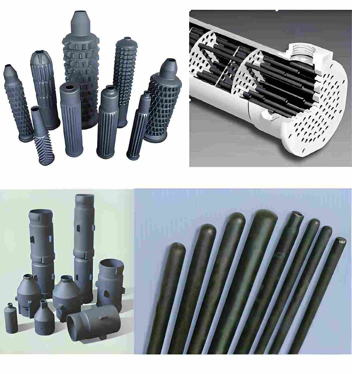
Zirsec offers a wide range of SiC components including tubes, beams, plates, crucibles, rollers, sealing rings, and custom mechanical parts for industrial, chemical, and semiconductor applications.
Can Zirsec provide customized sizes or shapes?
Yes. We support OEM and customized production based on your drawings, specifications, or working conditions.
Do you provide samples for testing?
Yes, sample orders are available for standard items. For custom-made components, small batch samples can be produced after design confirmation.
How can I request a quotation?
Simply fill out the contact form on this page with product type, quantity, and specifications. Our sales engineer will send you a detailed quotation within 24 hours.
Does Zirsec offer technical consultation or design assistance?
Absolutely. Our engineers provide material selection guidance, structural optimization, and technical support for your specific applications.
How does Zirsec ensure product quality?
All products undergo strict inspection procedures, including dimensional accuracy, density, strength, and corrosion resistance tests before delivery.
Tell us your requirements
Our technical engineer will reply with a custom solution and quotation within one working day.