Silicon carbide (SiC) is becoming a cornerstone material in modern semiconductor manufacturing, offering unmatched thermal stability and electrical performance.
- Why SiC? – Higher breakdown voltage, lower on‑resistance, and superior thermal conductivity.
- Key applications – SiC wafers, power MOSFETs, Schottky diodes, MEMS, and high‑temperature sensor packages.
- Design tips – Pay attention to lattice mismatch, thermal expansion, and surface finish.
- Supplier checklist – Purity ≥98 %, dimensional tolerance ±0.2 mm, 24‑hour stock availability, engineering support.
- Action – Contact ZIRSEC for custom SiC components or bulk stock at our Silicon Carbide product page.
1. The Real Reason Engineers Turn to SiC
When a device must operate above 200 °C or handle a few kilowatts of power in a compact footprint, silicon alone can’t compete. In our twelve‑year experience with high‑temperature equipment, we have repeatedly seen SiC deliver a 3‑5× increase in thermal conductivity (≈3.7 W·cm⁻¹·K⁻¹) and a band‑gap that stays stable up to 3.3 eV. The result is lower leakage current, higher switching frequency, and a dramatic reduction in heat‑sink size.
Thermal advantage
Typical silicon devices lose efficiency once the junction temperature exceeds 125 °C. SiC keeps the same performance at 300 °C, which means the same power density can be achieved with a 40‑60 % smaller cooling system. For a 1 kW inverter in an electric vehicle, that translates into a weight saving of roughly 2‑3 kg – a figure that matters on the production line.
Electrical advantage
SiC’s critical electric field is about ten times higher than silicon’s. That allows designers to create devices with lower on‑resistance (RDS(on)) while preserving a high breakdown voltage (VBD). In practice, a 1200 V SiC MOSFET can replace a 600 V silicon device, halving the number of series components in a power stack.
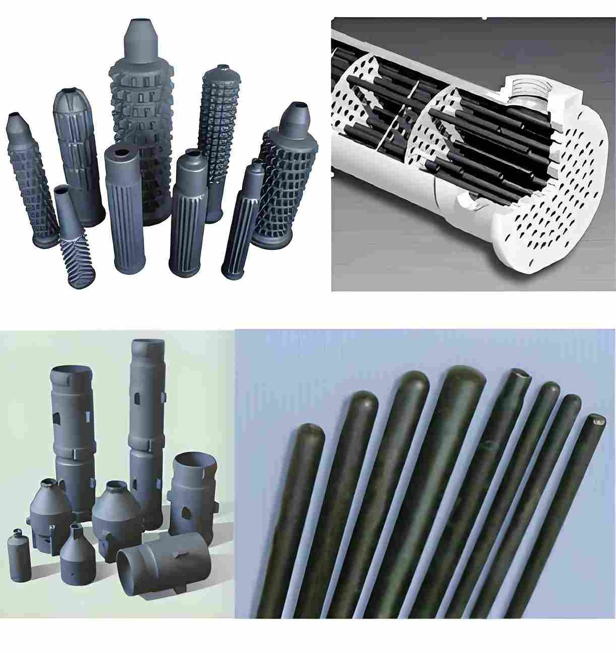
2. Core SiC Components in Semiconductor Production
Below is the list of parts we encounter most often when working with fabs, specialty equipment builders, and R&D labs.
2.1 SiC Wafers
Standard wafer diameters are 2‑inch, 3‑inch, and increasingly 4‑inch. The most common thickness is 350 µm, with ±0.02 mm flatness tolerance. Our customers in the United States and Germany ask for 99.9 % purity because any metallic impurity can cause premature breakdown during high‑frequency switching.
2.2 SiC Power Devices (MOSFETs, Schottky Diodes, JFETs)
Power MOSFETs built on SiC substrate exhibit a typical on‑resistance of 0.2–0.5 mΩ·cm², while a comparable silicon part sits at 2–3 mΩ·cm². Schottky diodes benefit from the low reverse recovery charge, enabling faster rectification in DC‑DC converters.
2.3 SiC MEMS and Sensors
High‑temperature pressure transducers and Hall‑effect sensors embed SiC membranes that survive 600 °C without creep. The mechanical strength (≥130 MPa) allows thin‑film structures (<50 µm) to survive repeated pressure cycles.
2.4 SiC Ceramic Packages and Heat Spreaders
For power modules that must be sealed against aggressive chemicals, we supply SiC ceramic plates and tubes that act as both structural support and heat spreader. Our standard plate (100 mm × 100 mm × 10 mm) can be ordered in a single‑day stock, with custom dimensions available within two weeks.
3. How SiC Is Integrated Into a Semiconductor Fab
In a typical silicon‑on‑insulator (SOI) line, SiC appears at three critical junctions: substrate preparation, device isolation, and final packaging.
3.1 Substrate Preparation
Before epitaxial growth, the SiC wafer is polished to a Ra ≤ 0.3 µm surface. Our polishing service uses a proprietary slurry that reduces subsurface damage to less than 5 nm – a level you normally see only in high‑end optical components.
3.2 Device Isolation
SiC’s high dielectric strength (≥3 MV·cm⁻¹) enables ion‑implant isolation without the need for thick field‑oxide layers. The process cuts the overall thermal budget by 20 %, which is crucial when bonding SiC chips to copper substrates.
3.3 Packaging and Thermal Management
After die‑sorting, we attach the SiC die to a copper‑molybdenum heat sink using a thin SiC ceramic interposer. The interposer’s coefficient of thermal expansion (≈4.5 × 10⁻⁶ K⁻¹) matches both copper and SiC, eliminating thermal stress during rapid temperature cycles.
4. Real‑World Case Studies – What Our Customers Have Achieved
4.1 High‑Power Automotive Inverter
A German EV supplier switched from 600 V silicon MOSFETs to 1200 V SiC devices on a 150 kW inverter platform. The SiC solution cut the inverter’s weight by 18 % and reduced the cooling fan speed by 35 %. The project saved the OEM roughly $120 k per vehicle in downstream logistics.
4.2 Semiconductor Etch Chamber
In a US wafer‑fab, the plasma‑etch chamber’s inner liner was upgraded to a SiC ceramic tube (Ø 150 mm, 2 m length). The tube’s resistance to fluorine‑based chemistries eliminated the need for periodic liner replacement, saving $45 k a year in downtime.
4.3 High‑Temperature Pressure Sensor for Steel Mills
A Japanese steel producer needed a pressure sensor that could survive 550 °C nitrogen atmosphere. We delivered a custom SiC MEMS sensor with a 0.15 mm thick membrane. After six months of operation, the sensor showed zero drift, whereas the previous silicon‑based sensor failed after 120 hours.
5. Design Checklist – What Engineers Must Verify Before Buying SiC
- Purity & Composition – SiC ≥ 98 % with minimal graphite inclusions; request a COA (Certificate of Analysis) for each batch.
- Dimensional Tolerance – ±0.2 mm for standard parts; tighter tolerances (±0.05 mm) are available with custom machining.
- Surface Roughness – Ra ≤ 0.8 µm for wafers, ≤ 3.2 µm for bulk plates; polishing improves electrical breakdown.
- Thermal Shock Resistance – Verify the part can survive a ±150 °C rapid cycle without cracking; our in‑house testing follows ASTM C1498.
- Documentation – Ensure MSDS, COA, and material safety certificates are attached to the shipment. This speeds up customs clearance in the US and EU.
6. Why Choose ZIRSEC As Your SiC Partner
We have been producing SiC ceramic tubes, plates, and custom parts for over 20 years. Our factory holds a 10,000 m² production area, with clean‑room machining stations that guarantee a 99.7 % first‑pass yield on tight‑tolerance orders. Here are three reasons why our clients keep coming back:
- Direct factory supply – No middle‑man mark‑up, and we can ship standard stock items within 24 hours.
- Full‑stack engineering support – Our in‑house engineers work with your CAD files, run finite‑element thermal analysis, and provide DFMEA reports before the first prototype.
- Flexible MOQ – From a single prototype (5 pcs) to a bulk run of 10,000 pcs, we keep lead times under eight weeks, and we offer expedited 4‑week service for critical projects.
7. Frequently Asked Questions (FAQ)
What is the typical cost of a 4‑inch SiC wafer?
Prices vary with purity and thickness, but a 4‑inch, 350 µm, 99.9 % SiC wafer usually ranges from $120 to $250 per piece for quantities of 50‑100 units.
Can SiC parts be coated with metal layers?
Yes. We regularly apply Ti/Au or Mo sputter layers for backside contacts. The coating thickness is limited to 5 µm to avoid cracking during thermal cycling.
How do I handle customs for SiC ceramic shipments?
Provide the commercial invoice, a copy of the COA, and the HS code 6817.00. Our logistics team can prepare a pre‑clearance packet that reduces clearance time to 1‑2 days in the US.
Is SiC compatible with lead‑free solders?
SiC itself is inert, but the copper interconnects should be tin‑silver‑copper (SAC305) to avoid intermetallic growth at temperatures above 250 °C.
8. Actionable Next Steps
If your next project demands high‑temperature reliability, lower parasitic losses, or a compact power architecture, start by requesting a free thermal‑analysis report from our engineering team. Upload your CAD drawing through the contact form on our website, and we will return a quotation, lead‑time estimate, and a draft of the risk‑mitigation plan within three business days.
Remember, a single SiC upgrade can shave hundreds of dollars off your total system cost by reducing the size of heat‑sinks, lowering the number of series components, and extending maintenance intervals. Let ZIRSEC help you turn those savings into a competitive edge.