Semiconductor manufacturing pushes materials and equipment to their limits. Cleanroom tools must run with ultra-low particle generation, excellent corrosion resistance and stable dimensions at elevated temperatures. Any unexpected contamination or drift in process conditions quickly translates into yield loss.
High-purity silicon carbide ceramics have become a valuable material class for selected semiconductor and cleanroom equipment components. With excellent thermal stability, chemical resistance and mechanical strength, high-grade silicon carbide (SiC) supports both front-end and back-end processes where metals and polymers reach their limits.
This article explains how high-purity silicon carbide ceramics fit into semiconductor manufacturing, where they are used in cleanroom equipment and what to consider when specifying them.

Semiconductor Manufacturing and Cleanroom Requirements
Semiconductor fabrication, as outlined in semiconductor device fabrication, combines complex process steps:
- Deposition (CVD, PVD, ALD)
- Etching (dry and wet)
- Thermal processing (diffusion, oxidation, annealing)
- Cleaning and surface preparation
- Wafer handling, transfer and packaging
Across these steps, cleanroom and process tools must meet three fundamental demands:
- Ultra-low contamination: minimal particle generation, metal ion contamination and outgassing.
- Chemical resistance: stability in aggressive chemistries such as acids, bases and reactive gases.
- Thermal and mechanical stability: precise control of temperature and geometry at process conditions.
Material selection for hot-zone parts, structural supports and fluid-contact surfaces is therefore critical for yield and process control.
Why High-Purity Silicon Carbide Ceramics Fit Semiconductor Equipment
Silicon carbide, described in silicon carbide, offers a set of properties that align well with semiconductor tool requirements when produced in high-purity grades:
- High temperature capability: maintains strength, stiffness and dimensional stability at elevated temperatures used in thermal processes.
- Good thermal conductivity: supports uniform temperature distribution in hot zones and process fixtures.
- Chemical resistance: compatible with many corrosive gases and liquids used in deposition, etching and cleaning.
- Low particle generation: dense, hard surfaces resist wear and micro-fracturing when properly finished.
- Dimensional stability: low creep and good resistance to thermal shock when designed correctly.
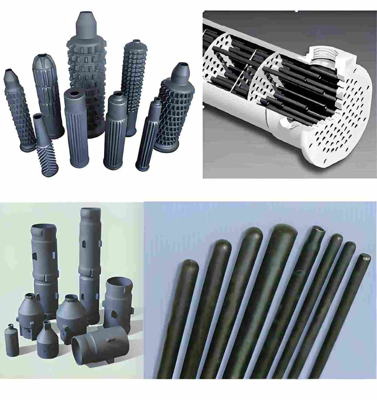
Zirsec’s industrial-grade silicon carbide products, such as silicon carbide plates, tubes and custom mechanical parts, can be engineered into semiconductor-related equipment where high wear, high temperature and cleanliness requirements converge.
Key Applications of Silicon Carbide Ceramics in Semiconductor Manufacturing
1. Furnace and Thermal Processing Components
Thermal processes such as oxidation, diffusion and annealing rely on precise temperature control and clean hot zones. High-purity SiC can be used for:
- Wafer support structures: carriers, trays and plates that hold wafers in vertical or horizontal furnaces.
- Hot-zone linings: SiC panels or tiles in areas exposed to high heat and reactive atmospheres.
- Tubes and shields: silicon carbide tubes used as radiant tubes, liners or protective shields in high-temperature sections.
These components benefit from silicon carbide’s combination of thermal conductivity and high-temperature strength, supporting stable thermal profiles and long service life.
2. Cleanroom Equipment and Handling Fixtures
Beyond process chambers, cleanroom equipment must handle wafers, carriers and components without generating particles or contamination:
- Precision plates and inserts: SiC plates used in fixtures that contact wafer carriers or process hardware.
- Mechanical parts: silicon carbide wear surfaces and guides in handling systems where abrasion is a concern.
Properly finished silicon carbide surfaces help reduce particle generation compared with softer materials that wear more quickly under repeated motion.
3. Corrosive Gas and Chemical Contact Areas
Some semiconductor tools operate with highly reactive gases or aggressive liquid chemistries. In selected locations, SiC ceramics can be used to:
- Protect metallic structures from corrosion at elevated temperature.
- Provide chemically stable surfaces in flow channels or distribution components.
While polymer-lined systems are common at lower temperatures, silicon carbide is more suited where temperature and mechanical loads are too high for plastics or elastomers.
Benefits of High-Purity Silicon Carbide Ceramics for Semiconductor Tools
Improved Stability and Uptime
Silicon carbide components maintain their geometry and mechanical integrity over long campaigns:
- Less drift in thermal profiles due to stable hot-zone parts.
- Longer service life before fixtures and liners require replacement.
- Reduced risk of sudden failures in high-temperature areas.
Lower Contamination Risk
In sensitive process steps, contamination control is everything. Properly specified SiC ceramics support this by:
- Minimising particle generation through hard, wear-resistant surfaces.
- Reducing metal ion contamination compared with some metal alloys.
- Providing chemically inert contact surfaces in critical zones.
Flexible Integration into Existing Designs
In many cases, silicon carbide components can be introduced into existing tool layouts:
- Retrofit of plates and inserts in fixtures where wear and temperature are problematic.
- Replacement of certain metallic elements with SiC parts in high-heat or high-corrosion subassemblies.
This allows incremental upgrades focusing on the most critical components rather than full tool redesign.
Engineering Considerations for Semiconductor Equipment Designers
1. Purity and Contamination Control
For semiconductor applications, not all silicon carbide grades are equal. When specifying SiC:
- Define purity requirements based on device node, process step and contamination budgets.
- Consider outgassing and extractables at operating temperature.
- Specify surface finish and cleaning protocols to support cleanroom use.
Industrial-grade SiC can be used effectively in support equipment, test rigs and non-front-end locations, while more stringent grades may be needed for direct process contact in advanced nodes.
2. Thermal and Mechanical Design
Silicon carbide behaves differently from metals under thermal and mechanical load:
- Use geometries that avoid sharp corners and large stress concentrations.
- Allow for thermal expansion matching with adjacent materials in fixtures and supports.
- Account for thermal cycling when sizing sections and supports.
Successful designs treat SiC as a high-performance ceramic with its own design rules, not as a one-to-one substitute for steel or aluminium.
3. Surface Finish, Flatness and Tolerance
In wafer handling and thermal processing, tight tolerances and surface quality matter:
- Specify flatness and thickness tolerance for plates and fixtures that contact wafers or carriers.
- Define surface roughness appropriate for cleanroom compatibility and particle control.
- Ensure repeatability across batches for multi-tool and multi-site deployments.
Zirsec’s experience with precision SiC mechanical parts supports the consistent tolerances needed in semiconductor-related equipment.
Case Example: Using Silicon Carbide Plates in a Thermal Test Rig
Background
A semiconductor equipment supplier needed a high-temperature test rig to validate new furnace hardware. Conventional metallic fixtures distorted and oxidised under repeated thermal cycles, introducing variability into test results.
Approach
- Replace key fixture surfaces with high-purity silicon carbide plates designed for the target temperature range.
- Optimise plate geometry and supports to distribute stress and allow for thermal expansion.
- Implement cleaning and handling procedures compatible with cleanroom-adjacent environments.
Results
- Test rig stability improved, with less drift in temperature profiles over repeated runs.
- Fixture life increased, reducing rebuild frequency and downtime.
- Data quality and repeatability improved, supporting faster development cycles.
FAQ – High-Purity Silicon Carbide Ceramics for Semiconductor Equipment
Q1. Are silicon carbide ceramics suitable for direct wafer contact?
In some applications, yes, but purity, surface finish and cleaning methods must be carefully controlled. Many users start by applying SiC to non-wafer-contact surfaces (fixtures, shields, supports) before considering direct wafer-contact roles, especially in advanced nodes.
Q2. Where is the most practical place to start using SiC in semiconductor manufacturing?
Start with high-temperature fixtures, shields and liners in thermal processes and test equipment, where existing materials show clear limitations in lifetime or stability. These locations often deliver visible benefits without requiring changes to core process recipes.
Q3. How does silicon carbide compare with quartz and alumina in semiconductor tools?
Quartz offers excellent purity and transparency but has lower mechanical strength at high temperatures. Alumina is a common technical ceramic with good chemical resistance. High-purity silicon carbide sits closer to the “high strength + high thermal conductivity” corner, making it attractive where mechanical loads, erosion and thermal gradients are more severe.
Q4. What information should I provide when requesting SiC components from Zirsec?
Provide process step, maximum and typical temperatures, ambient atmosphere or chemistry, required lifetime, contamination constraints, desired dimensions and current material issues. Drawings or models of the fixtures or components help translate these needs into SiC plate, tube or custom part designs.
Q5. Can silicon carbide components be cleaned and handled using standard cleanroom procedures?
Yes, in most cases. Silicon carbide is compatible with many standard cleaning chemistries, but cleaning protocols should be validated for each specific process and purity requirement. Surface finish and porosity must be matched to the cleaning and inspection methods used in your facility.
Designing or upgrading equipment for semiconductor manufacturing? Integrating high-purity silicon carbide ceramics into the right fixtures, hot zones and support structures can improve thermal stability, reduce contamination risks and support more reliable, repeatable processes in cleanroom environments.